
Welcome to next generation PVD.
Not just thin, thick film.
Wrought vs PVD (Physical Vapor Deposition)
Traditional medical device manufacturing is a multi-step technique that starts by foundry produced wrought materials undergoing hundreds of reductive steps involving die tooling, heating and lubricants. Many of these steps take place in un-clean environments until they reach the stage of the so-called medical tubing and wire. In cleaner spaces like medical device facilities, these materials undergo many steps of laser cutting, abrasive and electropolishing, and heat setting. Most of these steps remove material so that the final product has a small fraction of the initial mass. From the physical-chemistry standpoint, each step along the device manufacturing history leaves a footprint consisting of residual chemicals, structural defects and foreign inclusions. The relevance of these abnormalities depends on the expected mechanical performance and final device dimensions. In general, failure induced by these defects is related to size of the features, the mechanical workload and the corrosion exposure. Highly stressed devices of very small dimensions will be more prone to fail than larger counterparts, hence, the limit these materials and methods have when pursuing miniaturization.

Wrought Nitinol Stent Strut Image
Grain size 20-40μm, mean inclusion size 2,600nm, carbide and oxide inclusions.

PVD Nitinol Stent Strut Grain Level Image
Grain size 2.2μm (note the scale), mean inclusion size 45nm (<half as many), almost entirely carbide inclusions.
By contrast, Vactronix Scientific patented methodology is based on high vacuum, high energy build-up of alloys from basic donor materials. Elemental metal ions are deposited atom by atom from a plasma onto a substrate which serves as a template for the device in its final shape state. The resulting material is comparatively purer because of the elimination of tooling and manual labor steps. The process is tightly controlled by computer assistance eliminating human error variability. Also, our method parameters can be manipulated to affect crystal size, orientation and arrangement, therefore controlling the bulk microcrystalline structure. The resulting material has increased compositional purity and remarkable metallurgical properties. The inherent homogeneity makes it an ideal substrate for high-definition laser cutting. The small crystal size allows for smaller features that are metallurgically sound. Laser ablation beam control allows single digit micron tolerances that are difficult or impossible to maintain employing wrought materials. The following section will compare VS PVD and wrought materials to illustrate the enhanced capabilities of this novel technology.
Nitinol Tubing Process Comparison

Nitinol Component Process Comparison

Vactronix Scientific’s unique processing allows us to simplify the multi-step traditional manufacturing to only a few steps at a fraction of the time involved. By eliminating the multiple steps of heat setting and abrasive/corrosive polishing typically involved in vascular device manufacturing, this technology simplifies fabrication eliminating hand labor and reduces environmentally sensitive finish processes.
Excellent EP Finish
Combination of laser ablation and on-substrate EP process yields a new standard.
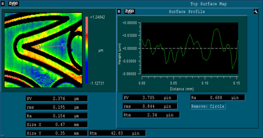

Holding ± single digit microns on specifications and surface roughness values under 1 μin is routine production at Vactronix Scientific every day.
We do Complicated

This capabilities demo part incorporates millimeter and micron features all in one monolithic design. This level of detail is impossible using conventional fabrication methods. Have a challenging design? Bring it on.

Because Vactronix’s technology is based on true 3D PVD, we are not limited to simple geometries. We routinely work with complex 3D shapes. Finally, a process that can meet your imagination.
Patent Protected
With over 350 patents and pending applications across 18 countries, we own our space. Vactronix Scientific continues to develop and enhance new capabilities every day. Our approachable R&D and supply agreements allow our customers to develop and own their device IP while benefitting from our worldwide patent protected processes.